


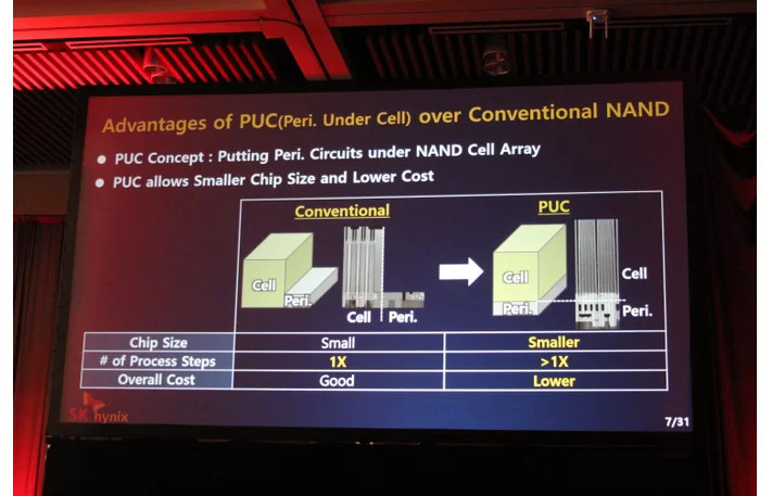
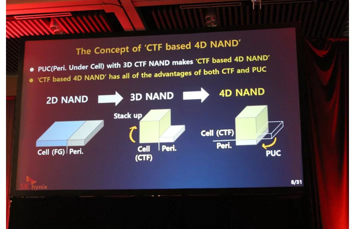
SK Hynix today launched the world’s first 96-Layer 512Gb CTF (Charge Trap Flash) based 4D NAND flash. Don’t let the name trick you – it’s still based on 3D TLC technology, but SK Hynix has gone and added a 4th dimension due to its pairing of charge trap flash technology in conjunction with PUC (Peri. Under Cell technology.
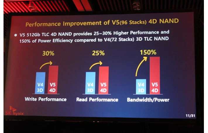
SK Hynix says that their approach is (obviously) better than the industry-wide 3D Floating Gate approach. The 4D NAND chip design results in a reduction of more than 30% in chip size, and increases bit productivity per wafer by 49% compared to the Company’s 72-Layer 512Gb 3D NAND. Moreover, the product has 30% higher write and 25% higher read performance. Also, its data bandwidth is doubled to an industry-leading (in size) 64KB. Data I/O (Input Output) speed reaches 1,200Mbps (Megabits/sec) at 1.2 V.
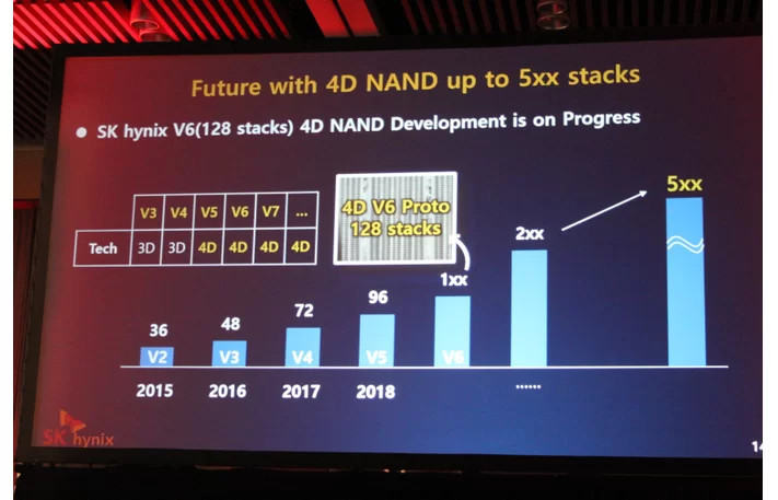
The plan in to introduce consumer products with up to 1 TB capacity alongside SK Hynix’s controllers and firmware; enterprise SSDs will follow in the first half of 2019, but Sk Hynix is still introducing 96-layer 1 Tb TLC and QLC memory chips in 2019.
“This 96-Layer CTF-based 4D NAND, with the industry’s top cost competitiveness and performance, will become a milestone in the Company’s NAND Flash business, as a platform in developing future products,” said vice president J.T. Kim, the Head of NAND Marketing. “The Company plans to start the early stage mass production of it within this year and further expand the production in M15 to actively respond to a variety of clients,” he added.

