


Xperi Corporation today announced that it entered into a new patent and technology license agreement with SK hynix, one of the world’s largest semiconductor manufacturers. The agreement includes access to Xperi’s broad portfolio of semiconductor intellectual property (IP) and a technology transfer of Invensas DBI Ultra 3D interconnect technology focused on next-generation memory.
“We are delighted to announce the extension of our long-standing relationship with SK hynix, a world-renowned technology leader and manufacturer of memory solutions,” said Craig Mitchell, President of Invensas, a wholly owned subsidiary of Xperi Corporation. “As the industry increasingly looks beyond conventional node scaling and turns toward hybrid bonding, Invensas stands as a pioneering leader that continues to deliver improved performance, power, and functionality, while also reducing the cost of semiconductors. We are proud to partner with SK hynix to further develop and commercialize our DBI Ultra technology and look forward to a wide range of memory solutions that leverage the benefits of this revolutionary technology platform.”
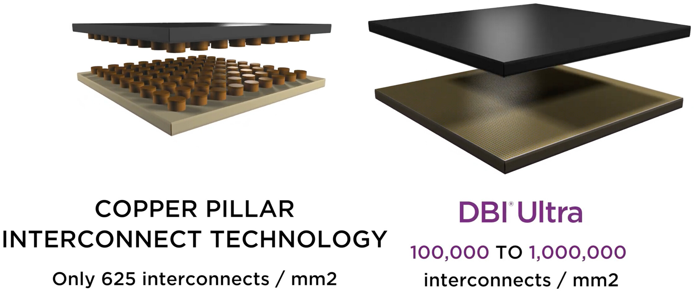
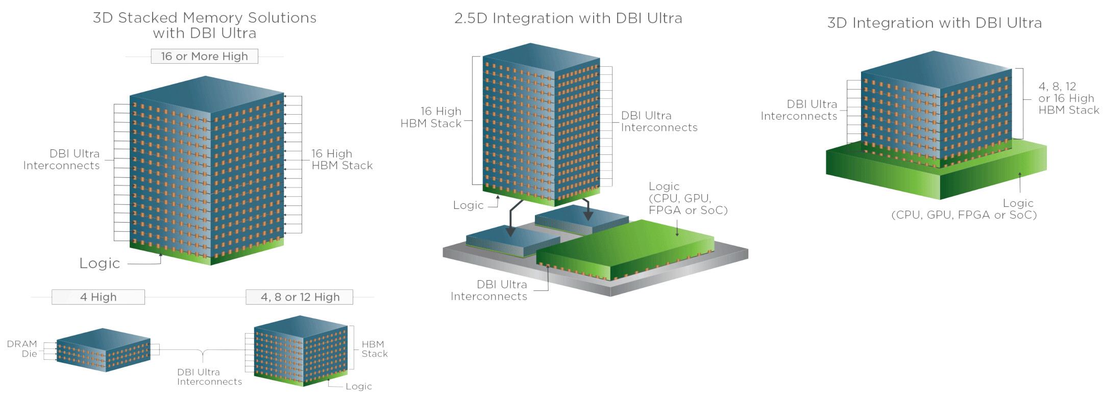
DBI Ultra is a patented die-to-wafer hybrid bonding 3D interconnect technology platform ushering in a new era of homogeneous and heterogeneous 3D integration. It allows the semiconductor industry to extend beyond Moore’s Law, providing unprecedented 2.5D and 3D integration flexibility. Among a wide range of applications, DBI Ultra makes it possible to manufacture 8-, 12- and even 16-high chip stacks while meeting the demanding packaging height and performance requirements for next generation, high-performance computing.
DBI wafer-to-wafer hybrid bonding, the predecessor to DBI Ultra, is already successfully incorporated into image sensors and RF components shipping in hundreds of millions of smartphones around the world. DBI Ultra is poised to realize similar success in 3D stacked memory as well as in 2.5D and 3D applications requiring the integration of memory with CPUs, GPUs, FPGAs, or SoCs. When optimized and applied by an industry leader like SK hynix, these technologies and the resulting semiconductor products will enable solutions for a wide range of applications from smartphones and smart homes to artificial intelligence (AI) and big data.
The terms and conditions of the agreement are confidential.

